
For the production of LED chips, the choice of substrate material is the primary consideration. Which suitable substrate should be used needs to be selected according to the requirements of the device and the LED device. At present, there are generally three kinds of materials on the market that can be used as substrates:
● Sapphire (Al2O3)
● Silicon (Si)
● Silicon carbide (SiC)[/url]
Typically, epitaxial layers of GaN-based materials and devices are grown primarily on sapphire substrates. Sapphire substrates have many advantages: First,
> For the production of LED chips, the choice of substrate material is the primary consideration. Which suitable substrate should be used needs to be selected according to the requirements of the device and the LED device. At present, there are generally three kinds of materials on the market that can be used as substrates:
Sapphire substrate
Typically, epitaxial layers of GaN-based materials and devices are grown primarily on sapphire substrates. Sapphire substrate has many advantages: first, the production technology of sapphire substrate is mature and the quality of the device is good; secondly, sapphire has good stability and can be used in high temperature growth process; finally, sapphire has high mechanical strength and is easy to handle and cleaning. Therefore, most processes generally use sapphire as the substrate. Figure 1 illustrates an LED chip made using a sapphire substrate.
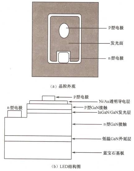
Figure 1 LED chip with sapphire as substrate
Using sapphire as a substrate also has some problems, such as lattice mismatch and thermal stress mismatch, which can create a large number of defects in the epitaxial layer and cause difficulties in the subsequent device processing process. Sapphire is an insulator with a resistivity greater than 1011Ω·cm at room temperature, in which case a device with a vertical structure cannot be fabricated; usually only n-type and p-type electrodes are fabricated on the upper surface of the epitaxial layer (as shown in Figure 1). Two electrodes are fabricated on the upper surface, which reduces the effective light-emitting area and increases the photolithography and etching processes in device manufacturing, resulting in lower material utilization and higher cost. Due to the difficulty of doping p-type GaN, a method of preparing metal transparent electrodes on p-type GaN is generally used to diffuse current to achieve uniform light emission. However, metal transparent electrodes generally absorb about 30% to 40% of light. At the same time, GaN-based materials have stable chemical properties and high mechanical strength, so it is not easy to etch them. Therefore, better equipment is required in the etching process. This will increase production costs.
The hardness of sapphire is very high, and its hardness is second only to diamond among natural materials, but it needs to be thinned and cut (from 400nm to about 100nm) in the manufacturing process of LED devices. Adding equipment to complete the thinning and cutting process adds another significant investment.
The thermal conductivity of sapphire is not very good (about 25W/(m·K) at 100℃). Therefore, when using LED devices, a large amount of heat will be conducted; especially for large-area high-power devices, thermal conductivity is a very important consideration. In order to overcome the above difficulties, many people try to grow GaN optoelectronic devices directly on silicon substrates to improve thermal and electrical conductivity.
silicon substrate
At present, some LED chips use silicon substrates. The chip electrode of the silicon substrate can adopt two contact methods, namely L-contact (Laterial-contact, horizontal contact) and V-contact (Vertical-contact, vertical contact), hereinafter referred to as L-type electrode and V-type electrode. Through these two contact methods, the current inside the LED chip can flow laterally or vertically. Since the current can flow longitudinally, the light-emitting area of the LED is increased, thereby improving the light-extraction efficiency of the LED. Because silicon is a good conductor of heat, the thermal conductivity of the device can be significantly improved, thereby extending the life of the device.
Silicon carbide substrate
The LED chip electrode of the silicon carbide substrate (CREE company in the United States specially uses SiC material as the substrate) is an L-shaped electrode, and the current flows longitudinally. The electrical conductivity and thermal conductivity of the device made of this substrate are very good, which is favorable for making a large-area high-power device. An LED chip using a silicon carbide substrate is shown in Figure 2.
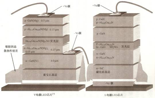
Figure 2 LED chip using sapphire substrate and silicon carbide substrate[/url],
The thermal conductivity of silicon carbide substrates (the thermal conductivity of silicon carbide is 490W/(m·K)) is more than 10 times higher than that of sapphire substrates. Sapphire itself is a poor conductor of heat, and the bottom of the device needs to be solidified with silver paste, which also has poor heat transfer performance. The chip electrodes using a silicon carbide substrate are L-shaped, and the two electrodes are distributed on the surface and bottom of the device, and the heat generated can be directly dissipated through the electrodes; at the same time, this substrate does not require a current diffusion layer, so the light will not be affected by the current. The material of the diffusion layer absorbs, which in turn improves the light extraction efficiency. However, compared with the sapphire substrate, the manufacturing cost of silicon carbide is relatively high, and the corresponding cost needs to be reduced to realize its commercialization.
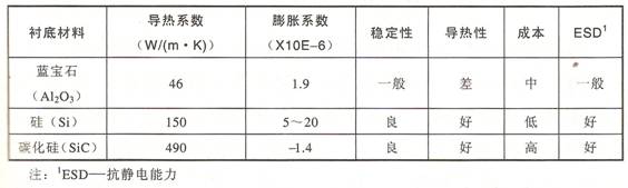
Performance comparison of three substrates
The previous content introduces three kinds of substrate materials commonly used to make LED chips. The comprehensive performance comparison of these three substrate materials can be seen in Table 1.
In addition to the above three commonly used substrate materials, GaAS, AlN, ZnO and other materials can also be used as substrates, which are usually selected and used according to the needs of the design.
Evaluation of substrate materials
1. The structure of the substrate and the epitaxial film is matched: the crystal structure of the epitaxial material and the substrate material is the same or similar, the lattice constant mismatch is small, the crystal performance is good, and the defect density is low;
2. Matching the thermal expansion coefficient of the substrate and the epitaxial film: the matching of the thermal expansion coefficient is very important. The large difference in the thermal expansion coefficient between the epitaxial film and the substrate material may not only reduce the quality of the epitaxial film, but also cause heat during the operation of the device. damage to the device;
3. The chemical stability of the substrate and the epitaxial film should be matched: the substrate material must have good chemical stability, and it is not easy to decompose and corrode in the temperature and atmosphere of epitaxial growth, and the quality of the epitaxial film cannot be deteriorated due to the chemical reaction with the epitaxial film;
4. The difficulty of material preparation and the level of cost: Considering the needs of industrial development, the preparation requirements of substrate materials are simple and the cost should not be very high. The substrate size is generally not less than 2 inches.
There are many substrate materials currently used for GaN-based LEDs, but there are currently only two substrates that can be used for commercialization, namely sapphire and silicon carbide substrates. Other substrates such as GaN, Si, and ZnO are still in the research and development stage, and there is still a distance from industrialization.
Gallium Nitride:
The most ideal substrate for GaN growth is GaN single crystal material, which can greatly improve the crystal quality of the epitaxial film, reduce the dislocation density, increase the working life of the device, improve the luminous efficiency, and improve the working current density of the device. However, it is very difficult to prepare GaN bulk single crystals, and so far there is no effective method.
Zinc oxide:
ZnO is a candidate substrate for GaN epitaxy because of the striking similarities between the two. The two have the same crystal structure, very small lattice recognition, and close band gaps (small energy band discontinuity value and small contact barrier). However, the Achilles heel of ZnO as a GaN epitaxial substrate is that it is easily decomposed and corroded in the temperature and atmosphere of GaN epitaxial growth. At present, ZnO semiconductor materials cannot be used to manufacture optoelectronic devices or high-temperature electronic devices, mainly because the material quality cannot reach the device level and the problem of P-type doping has not been truly solved, and the equipment suitable for the growth of ZnO-based semiconductor materials has not been successfully developed.
sapphire:
The most common substrate for GaN growth is Al2O3. Its advantages are good chemical stability, no visible light absorption, moderate price, and relatively mature manufacturing technology. Although the poor thermal conductivity is not exposed to obvious deficiencies in the small current operation of the device, the problem is very prominent in the high current operation of the power type device.
Silicon carbide:
SiC as a substrate material is second only to sapphire, and there is no third substrate for the commercial production of GaN LEDs. SiC substrate has good chemical stability, good electrical conductivity, good thermal conductivity, no absorption of visible light, etc., but its shortcomings are also very prominent. In addition, the SiC substrate absorbs ultraviolet light below 380 nanometers and is not suitable for the development of ultraviolet LEDs below 380 nanometers. Due to the beneficial electrical conductivity and thermal conductivity of SiC substrate, it can better solve the problem of heat dissipation of power GaN LED devices, so it occupies an important position in the field of semiconductor lighting technology.
Compared with sapphire, the lattice matching of SiC and GaN epitaxial films is improved.


